

Registrazione Unisciti a GRATUITO


1 / 3
DDR3 Specifiche del modulo di memoria UDIMM
| Model No. : | NSO4GU3AB |
|---|
Shenzhen, Guangdong, China
- Produttore
- Compagnia commerciale
- Fornitore Oro

- Certificazione della piattaforma

- Expo online


Descrizione del prodotto
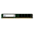
4GB 1600MHz 240 pin ddr3 udimm
Cronologia delle revisioni
|
Revision No. |
History |
Draft Date |
Remark |
|
1.0 |
Initial Release |
Apr. 2022 |
|
![]()
Tabella delle informazioni di ordinazione
|
Model |
Density |
Speed |
Organization |
Component Composition |
|
NS04GU3AB |
4GB |
1600MHz |
512Mx64bit |
DDR3 256Mx8 *16 |
Descrizione
Hengstar DIMMS DDR3 SDRAM non infastiditi (moduli di memoria in linea Dram a doppia frequenza dati DRAM) sono moduli di memoria di funzionamento ad alta velocità a bassa potenza che utilizzano dispositivi DDR3 SDRAM. NS04GU3AB è un prodotto DDR3 DDR3-1600 DDR3-1600 DDR3-1600 a due ranghi X da 512 m, basato su sedici componenti FBGA da 256 m a 8 bit. L'SPD è programmato per la latenza standard JEDEC DDR3-1600 di 11-11-11 a 1,5 V. Ogni Dimm a 240 pin utilizza dita di contatto d'oro. Il DIMM non infranto SDRAM è destinato all'uso come memoria principale quando installato in sistemi come PC e workstation.
Caratteristiche
Perca potenza: VDD = 1.5V (da 1.425v a 1.575V)
VDDQ = 1.5V (da 1.425v a 1.575V)
80000MHz FCK per 1600 MB/sec/pin
8 banca interna indipendente
Latenza CAS programmabile: 11, 10, 9, 8, 7, 6
Latenza additiva programmabile: 0, Cl - 2 o Cl - 1 Clock
8-BIT Pre-FETCH
Lunghezza per scopi: 8 (interleave senza limiti, sequenziale con l'indirizzo iniziale solo "000"), 4 con TCCD = 4 che non consente una lettura o scrittura senza soluzione di continuità [al volo usando A12 o MRS]
Dati differenziali BIBI STROBE
Calibrazione interiore (auto); Auto -calibrazione interna tramite PIN ZQ (RZQ: 240 ohm ± 1%)
La risoluzione del dado utilizzando ODT PIN
Periodo di aggiornamento della media 7,8US a meno di TCASE 85 ° C, 3,9US a 85 ° C <tcase <95 ° C
Reimposta asincrona
Resotta da unità di output dati regolabile
Topologia fly-by
pcb: altezza 1,18 "(30 mm)
Rohs conforme e senza alogeno
Parametri di temporizzazione dei tasti
|
MT/s |
tRCD(ns) |
tRP(ns) |
tRC(ns) |
CL-tRCD-tRP |
|
DDR3-1600 |
13.125 |
13.125 |
48.125 |
2011/11/11 |
Tabella degli indirizzi
|
Configuration |
Refresh count |
Row address |
Device bank address |
Device configuration |
Column Address |
Module rank address |
|
4GB |
8K |
32K A[14:0] |
8 BA[2:0] |
2Gb (256 Meg x 8) |
1K A[9:0] |
2 S#[1:0] |
Descrizioni dei pin
|
Symbol |
Type |
Description |
|
Ax |
Input |
Address inputs: Provide the row address for ACTIVE commands, and the column |
|
BAx |
Input |
Bank address inputs: Define the device bank to which an ACTIVE, READ, WRITE, or |
|
CKx, |
Input |
Clock: Differential clock inputs. All control, command, and address input signals are |
|
CKEx |
Input |
Clock enable: Enables (registered HIGH) and disables (registered LOW) internal circuitry |
|
DMx |
Input |
Data mask (x8 devices only): DM is an input mask signal for write data. Input data is |
|
ODTx |
Input |
On-die termination: Enables (registered HIGH) and disables (registered LOW) |
|
Par_In |
Input |
Parity input: Parity bit for Ax, RAS#, CAS#, and WE#. |
|
RAS#, |
Input |
Command inputs: RAS#, CAS#, and WE# (along with S#) define the command being |
|
RESET# |
Input |
Reset: RESET# is an active LOW asychronous input that is connected to each DRAM and |
|
Sx# |
Input |
Chip select: Enables (registered LOW) and disables (registered HIGH) the command |
|
SAx |
Input |
Serial address inputs: Used to configure the temperature sensor/SPD EEPROM address |
|
SCL |
Input |
Serial |
|
CBx |
I/O |
Check bits: Used for system error detection and correction. |
|
DQx |
I/O |
Data input/output: Bidirectional data bus. |
|
DQSx, |
I/O |
Data strobe: Differential data strobes. Output with read data; edge-aligned with read data; |
|
SDA |
I/O |
Serial |
|
TDQSx, |
Output |
Redundant data strobe (x8 devices only): TDQS is enabled/disabled via the LOAD |
|
Err_Out# |
Output (open |
Parity error output: Parity error found on the command and address bus. |
|
EVENT# |
Output (open |
Temperature event: The EVENT# pin is asserted by the temperature sensor when critical |
|
VDD |
Supply |
Power supply: 1.35V (1.283–1.45V) backward-compatible to 1.5V (1.425–1.575V). The |
|
VDDSPD |
Supply |
Temperature sensor/SPD EEPROM power supply: 3.0–3.6V. |
|
VREFCA |
Supply |
Reference voltage: Control, command, and address VDD/2. |
|
VREFDQ |
Supply |
Reference voltage: DQ, DM VDD/2. |
|
VSS |
Supply |
Ground. |
|
VTT |
Supply |
Termination voltage: Used for control, command, and address VDD/2. |
|
NC |
– |
No connect: These pins are not connected on the module. |
|
NF |
– |
No function: These pins are connected within the module, but provide no functionality. |
Note : La tabella di descrizione del pin seguente è un elenco completo di tutti i possibili pin per tutti i moduli DDR3. Tutti i pin elencati possono non essere supportato su questo modulo. Vedere le assegnazioni dei pin per informazioni specifiche per questo modulo.
Diagramma a blocchi funzionale
4 GB, modulo 512mx64 (2Rank di X8)


Dimensioni del modulo
Vista frontale

Vista frontale

Appunti:
1. tutte le dimensioni sono in millimetri (pollici); Max/min o tipico (tipo) dove indicato.
2.Tolerance su tutte le dimensioni ± 0,15 mm se non diversamente specificato.
3. Il diagramma dimensionale è solo a riferimento.


Shenzhen, Guangdong, China
- Produttore
- Compagnia commerciale
- Fornitore Oro
- Certificazione della piattaforma
- Expo online
Invia la tua richiesta a questo fornitore